I recently purchased a « non working » TC Electronic System 6000, here’s a few notes of what I found while trying to fix it.
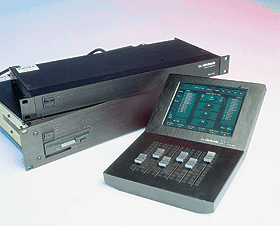
The TC Electronic System 6000 is based on two units:
- The Mainframe with a floppy disk drive and a PCMCIA slot
- The Remote + Icon
In my case, the remote unit works fine: the system boots properly, shows the Windows NT4 splashscreen and then the M6000 GUI.
The Mainframe unit is another story: the front panel is fixed red and.. stays red.
During a normal boot process, it’s supposed to access the floppy disk drive and the LED turns green once the boot is complete.
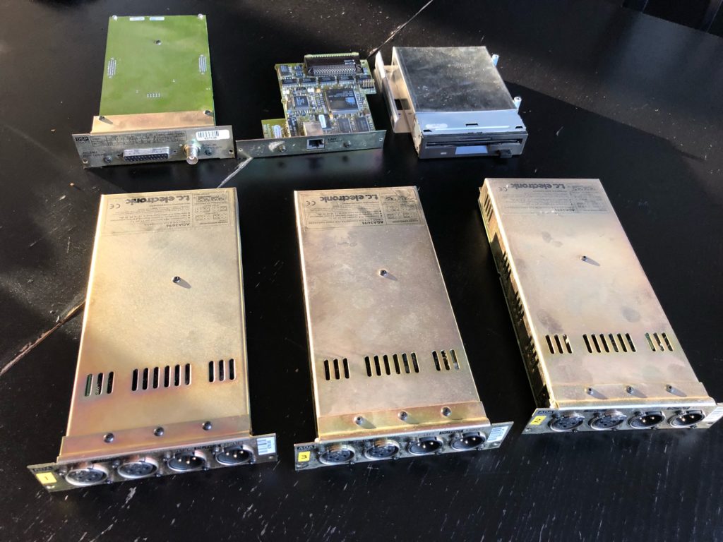
The Mainframe parts
The mainframe unit contains the following parts:
- A power supply
- A floppy disk drive
- The AES/DSP cartridge
- The AD/DA cartridge(s)
- A network card
- The mainboard
Power supply
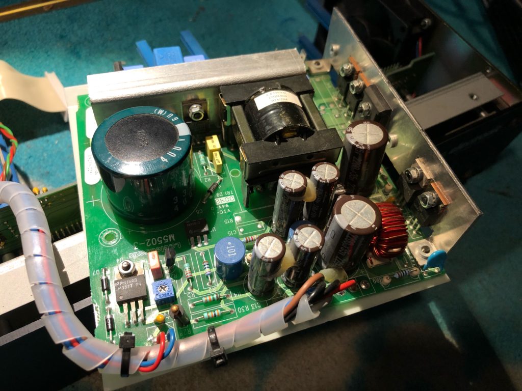
The power supply unit delivers +/-5V and +/-20V:
- Black / Red 5V
- Black / Gray -5,2V
- Black / Brown 20,5V
- Black / Blue -21V
There’s also two wires connected to the fan (and a temperature probe): red/blue 5V. The potentiometer is probably used to adjust the temperature level triggering the fan.
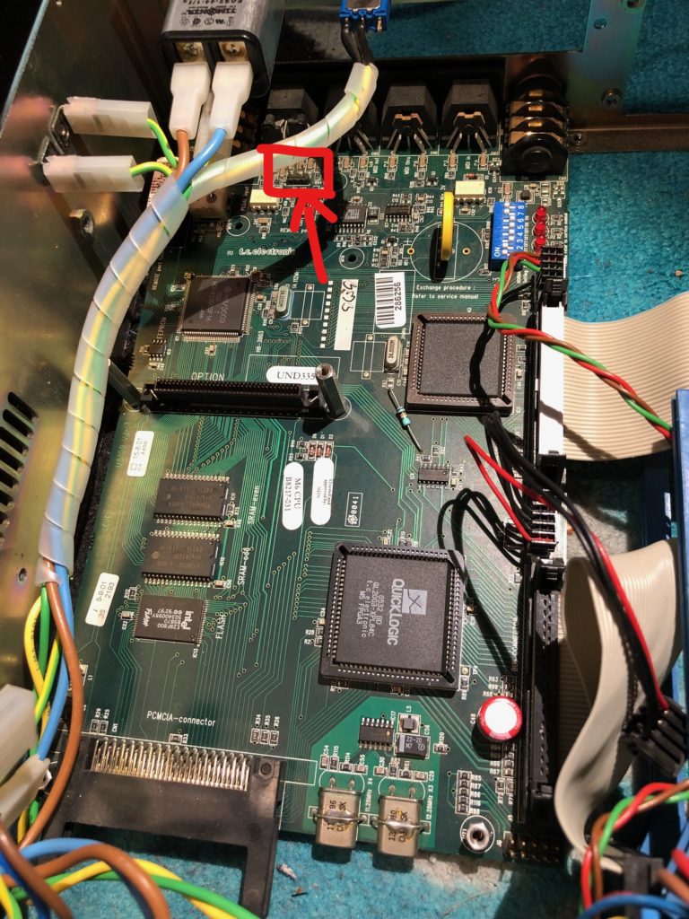
Motherboard
Taking a look inside the unit shows the following:
- the internal DIP switches are in default position: ON ON OFF OFF OFF OFF ON ON
- the LEDs are in the following state: ON OFF OFF BLINK
I tried booting without additional units (AD/DA, DSP, floppy disk drive, ethernet card) without success.
I also tried replacing the floppy disk drive with a Gotek floppy to USB emulator. This actually didn’t worked, the floppy drive is still not accessed. Since the Gotek drive has many configuration options it’s hard to tell if it’s normal.
The motherboard hosts:/
- H8/3003, 16bits microcontroller
- A QuickLogic FPGA
- A floppy disk drive controller
- Two RAM chips
- A Flash chip
As far as I understand the system, the H8 is in charge of the boot process: read from the floppy disk drive (through the floppy disk drive controller) firmware updates. If found, flash the H8 bootloader itself (on the Flash chip) or the FPGA.
At this point, I had to go deeper and try to understand how the motherboard actually works. TC Electronic does not provide any schematic nor service manual, but by searching deeper I found the Motherboard schematic here: https://service-tcgroup.tcelectronic.com/files/tech_service/s6000/schematics/cpu-m5100-3a2.pdf
Reverse & Serial port
The bootloader firmware « M6bv20.ins » seems to contain debug strings, so there’s may be some serial output for debugging purpose.
The schematics shows that the H8 has two serial ports, and following these brings us to the DIN 7 « Remote port » at the back of the unit. The Serial port 1 (Tx0/Tx0) is connected as follow:
- pin 2 : GND
- pin 3: Tx
- pin 4: Rx+
- pin 5: Rx-
Moreover, the unused JP3 connector also exhibits the same serial port and really looks like a debug interface:
- pin 1 (closest to the board corner): GND
- pin 2 : Rx
- pin 3: Tx
I used an USB to serial adapter to connect to this port, hoping for a terminal connection (or at least debug strings). Sadly, the port seems to be inactive, at least at this part of the boot process.
Reverse & DIP switches
The motherboard schematics provides interesting information on the DIP switches usage:
| DIP # | ON | OFF |
| 1 (sw1A) | Send boot_cs to inernal flash cs (Chip Select) | |
| 2 (sw1B) | Send pcmcia_mem_cs to fpga pcm_bus_cs | |
| 3 (sw1C) | Send boot_cs to fpga pcm_bus_cs | |
| 4 (sw1D) | Send pcmcia_mem_cs to flash cs | |
| 5 (sw1E) | Connect H8 MD2 to GND | Put 5V on the H8 MD2 |
| 6 (sw1F) | Put 5V on the H8 MD0/MD1 | Connect H8 MD0/MD1 to GND |
| 7 (sw1G) | Connect sram_cs to RAM chips CS | Disable external RAM |
| 8 (sw1H) | Connect flash_cs to FLASH | Disable Flash |
According the the schematic labels we also learn:
- Set switches 1 and 2 to ON for ROM boot
- Set switches 3 and 4 to ON for « CARD » boot (pcmcia sram)
- Set switches 5 and 6 to ON for 8bits operation (16 bits otherwise)
ROM boot: (1&2)
The switches 1 and 2 are ON by default, which makes sense: the unit is supposed to boot on the ROM. When switch 1 is set to ON, the boot_cs (a signal used to enable/disable a chip, thus select who’s going to read data sent on a bus) is connected to the flash memory cs. The switch 2 connects the pcmcia_mem_cs (again, a signal used to enable access to the PCMCIA) to the FPGA. I guess the FPGA is in charge of driving the PCMCIA.
During boot: read flash memory
After boot, when using PCMCIA: use pcmcia
CARD boot: (3&4)
When set to ON, the 3 and 4 switches enable the CARD boot. Thanks to the 3rd switch, boot_cs signal is sent to the FPGA pcm_bus_cs, which probably propagates this to the PCMCIA slot. During boot, the PCMCIA card is then enabled. The switch 4, connects the pcmcia_mem_cs to the external flash cs, thus when accessing the PCMCIA slot after the boot process, the unit will actually read the external flash.
During boot: read pcmcia
After boot, when using PCMCIA: use external flash
Here I learned something protentially fixing my issue: I suspect the bootloader to be corrupted and thus not accessing the floppy disk drive. If if use CARD boot mode, with a pcmcia sram memory card contaning the boot image (« M6bv20.ins ») raw written on it, I may actually bypass the flash memory issue. I found some technical documentation explaining that the M6bv20.ins should be copied to a floppy disk, then flashed on the SRAM pcmcia using a M5000 unit (« Wizard to disk » tool).
8/16 bits (5&6):
Switches 5 and 6 interacts with the H8/3003 MD0, MD1 and MD3 pins.
According to the microcontroller documentation (https://datasheet.octopart.com/HD6413003TF16-Renesas-datasheet-11768175.pdf):
| MD0 / MD1 | MD 2 | H8 Operation mode |
| 0 | 0 | not allowed |
| 0 | 1 | mode 4 |
| 1 | 0 | mode 3 |
| 1 | 1 | not allowed |
Mode 3: Address pins A23 to A0 are enabled, permitting access to a maximum 16-Mbyte address space. The initial bus mode after a reset is 8 bits, with 8-bit access to all areas. If at least one area is designated for 16-bit access in ABWCR, the bus mode switches to 16 bits.
Mode 4: Address pins A23 to A0 are enabled, permitting access to a maximum 16-Mbyte address space. The initial bus mode after a reset is 16 bits, with 16-bit access to all areas. If all areas are designated for 8-bit access in ABWCR, the bus mode switches to 8 bits.
So clearly, these two switches are used to select 8 or 16bits memory addressing, keeping the default position to 16bits (off/off) is a good option since I do not plan to rewrite the whole firmware 🙂
External RAM (7)
When OFF, switch 7 disables the two external RAM chips, thus the H8 CPU can only use its internal memory. Clearly we don’t want this and we’ll let this switch to ON.
External Flash (8)
When OFF, switch OFF disables the Flash chip during flash operations. Again, we don’t want this and we’ll let this switch to ON.
Reverse & JTAG
The J6 connector is a JTAG debug interface, connected to the FPGA. It’s probably used to load the fpga firmware in the factory. Since I don’t have a JTAG probe (and passing sniffing is pointless), it’s currently useless.
Factory setup
As far as I currently understand the motherboard, I suppose that:
- the H8 firmware is loaded using the DIP Switch 3&4 and a PCMCIA card with the bootloader firmware written. Thus, the H8 boots properly and is then able to « update » the bootloader using the floppy disk, writing the program on the flash.
- the FPGA firmware is loaded using the JTAG interface, probably prior to the H8, since the FPGA seems to be in charge of controlling the floppy disk driver.
Host Bus interface
I used my Salaea probe to watch traffic from the motherboard to the Host Bus Interface card. I didn’t tried to decode the whole traffic, but clearly there’s some.
Flash memory bus
I’m currently trying to scan the accesses to the flash memory bus, hoping it may help me to find what’s going on. The best place to sniff the bus seems to be the Ethernet card: the card shares the BUS with the flash chip, and the connector can easily be used to connect my probes. I’ll have to collect 3 bits lanes for each run and then reassemble, my Salaea is the 4 channel version. 1 channel will be used for the Clock (pin 43) and the 3 others for data.
Une réponse sur “Going deeper on the M6000”